
Modeling of Crystal Growth from the Melt
Modeling of crystal growth from the melt is one of the priority activities of our company. Working with industrial companies and participating in research projects, we have gained profound experience in optimization of bulk crystal growth by the Czochralski (CZ), Bridgman, vertical gradient freezing (VGF), and floating zone (FZ) techniques. Using numerical simulation, our research team works with the growth equipment manufacturers at the design stage and, later on, at the calibration stage, which considerably speeds up the design process, cuts test run costs, and allows our customers to get a crystal with the optimal parameters. Furthermore, subsequent shrinking of quality requirements for semiconductor and optical crystals on the market necessitates day-to-day tuning of the growth technology. Such tuning can also be provided with much more efficiency using numerical modeling.
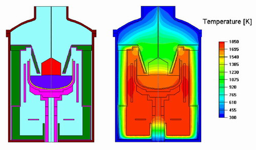 Fig. 1.
Example of global heat transfer analysis in 400 mm CZ Si growth
(furnace geometry is from Journal of Crystal Growth 229-2001-p.17).
|
For our industrial and research partners, we propose the following services:
- global heat transfer modeling in growth systems for optimization of the whole geometry, heat shields, and heaters;
- analysis of thermal-elastic stresses and dislocation generation in the crystal with the calculation of the crystallization front geometry;
- prediction of defect characteristics (voids, oxygen precipitates) in silicon crystals;
- calculations of impurity transport in the gas and melt for predicting the concentrations in the crystal;
- advanced analysis of melt and gas convection with the application of turbulence models and direct numerical simulation (LES, DNS) of 3D unsteady flows, using parallel computing on a cluster;
- delivery and wide support of customized versions of the Crystal Growth Simulator (CGSim) package for "in-house" modeling of customers.
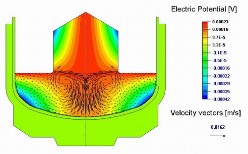 Fig. 2.
Example of application of cusp DC magnetic field in 400 mm CZ Si
growth. |
The models incorporated into the software are successfully verified for silicon Si, gallium arsenide GaAs, indium phosphide InP, sapphire, silicon germanium SiGe, and other semiconductor and optical crystals.
The Flow Module of CGSim package, containing options for parallel computations using a cluster of PCs, was developed with the financial support of The Foundation for Assistance to Small Innovative Enterprises (FASIE).
Selected References
2004
"3D Computations of Melt Convection and Crystallization Front Geometry during VCz GaAs Growth" O.V. Smirnova, V.V. Kalaev, Yu.N. Makarov, Ch. Frank-Rotsch, M. Neubert, P. Rudolph, J. Crystal Growth 266 (2004) pp 67-7320.
"Simulation of Heat Transfer and Melt Flow in Czochralski Growth of Si1-xGex Crystals", O.V. Smirnova, V.V. Kalaev, Yu.N. Makarov, N.V. Abrosimov, H. Riemann, J. Crystal Growth 266 (2004) pp. 74-80
"Advances in the simulation of heat transfer and prediction of the melt-crystal interface shape in silicon CZ growth", D.P. Lukanin, V.V. Kalaev, Yu. N. Makarov, T. Wetzel, J. Virbulis, and W. von Ammon, J. Crystal Growth, 266/1-3 (2004) pp. 20 - 27
"Parallel Simulation of Czochralski crystal growth", D. Lukanin, V. Kalaev, A. Zhmakin, Lecture Notes in Computer Science, Vol. 3019 (2004) pp. 469 - 474
"3D unsteady numerical analysis of conjugate heat transport and turbulent/laminar flows in LEC growth of GaAs crystals", O.V. Smirnova and V.V. Kalaev, International Journal of Heat and Mass Transfer 47 (2004) pp. 363-371
2003
"Variations of solid-liquid interface in the BGO low thermal gradients Cz growth for diffuse and specular crystal side surface", V.S. Yuferev, O.N. Budenkova, M.G. Vasiliev, S.A. Rukolaine, V.N. Shlegel, Ya.V. Vasiliev, A.I. Zhmakin, J. Crystal Growth 253 (2003) 383-397
"Modeling of point defect formation in silicon monocrystals", V. A. Zabelin and V. V. Kalaev, Microelectronic Engineering 69 (2003) pp. 641-645
"Modeling Analysis of Liquid Encapsulated Czochralski Growth of GaAs and InP Crystals", E.V.Yakovlev, V.V. Kalaev, E.N. Bystrova, O.V. Smirnova, Yu.N. Makarov, Ch. Frank-Rotsch, M. Neubert, P. Rudolph, Crystal Research and Technology, 38, No. 6 (2003) pp. 506-514
"Prediction of bulk defects in CZ Si crystals using 3D unsteady calculations of melt convection", V.V. Kalaev, D.P. Lukanin, V.A. Zabelin, Yu.N. Makarov, J. Virbulis, E. Dornberger, W. von Ammon, Materials Science in Semiconductor Processing, 5/4-5 (2003) pp. 369-373
"Global heat and mass transfer in vapor pressure controlled Czochralski growth of GaAs crystals", E.V. Yakovlev, V.V. Kalaev, I.Yu. Evstratov, Ch. Frank, M. Neubert, P. Rudolph, Yu.N. Makarov, J. Crystal Growth, 252/1-3 (2003) pp. 26-36
"Modeling analysis of vCZ growth of GaAs bulk crystals using 3D unsteady melt flow simulations", E.V. Yakovlev, O.V. Smirnova, E.N. Bystrova, V.V. Kalaev, Ch. Frank-Rotsch, M. Neubert, P. Rudolph, Yu.N. Makarov, J. Crystal Growth, 250/1-2 (2003) pp. 195-202
"Prediction of the melt/crystal interface geometry in liquid encapsulated Czochralski growth of InP bulk crystals", E.N. Bystrova, V.V. Kalaev, O.V. Smirnova, E.V. Yakovlev, Yu.N. Makarov, J. Crystal Growth, 250/1-2 (2003) pp. 189-194
"Analysis of magnetic field effect on 3D melt flow in CZ Si growth", N.G. Ivanov, A.B. Korsakov, E.M. Smirnov, K.V. Khodosevitch, V.V. Kalaev, Yu.N. Makarov, E. Dornberger, J. Virbulis, W. von Ammon, J. Crystal Growth, 250/1-2 (2003) pp. 183-188
"Calculation of bulk defects in CZ Si growth: impact of melt turbulent fluctuations", V.V. Kalaev, D.P. Lukanin, V.A. Zabelin, Yu.N. Makarov, J. Virbulis, E. Dornberger, W. von Ammon, J. Crystal Growth, 250/1-2 (2003) pp. 203-208
"Gas flow effect on global heat transport and melt convection in Czochralski silicon growth", V. V. Kalaev, I. Yu. Evstratov, Yu. N. Makarov, J. Crystal Growth, 249/1-2 (2003) pp. 87-99
2002
"Numerical study of 3D unsteady melt convection during industrial-scale CZ Si-crystal growth", I.Yu. Evstratov, V.V. Kalaev, A.I. Zhmakin, Yu.N. Makarov, A.G. Abramov, N.G. Ivanov, A.B. Korsakov, E.M. Smirnov, E. Dornberger, J. Virbulis, E. Tomzig, W. von Ammon, Journal of Crystal Growth 237-239 (2002) 1757-1761
"Modeling of impurity transport and point defect formation during Cz Si crystal growth", V.V. Kalaev, V.A. Zabelin, Yu.N. Makarov, Solid State Phenomena 82-84 (2002) pp. 41-46
2001
"Modeling analysis of unsteady three-dimensional turbulent melt flow during Czochralski growth of Si crystals", I.Yu. Evstratov, V.V. Kalaev, A.I. Zhmakin, Yu.N.Makarov, A.G. Abramov, N.G. Ivanov , E.M. Smirnov, E. Dornberger, J. Virbulis, E. Tomzig, W. v.Ammon, Journal of Crystal Growth 230 (2001) pp. 22-29
"Global model of Czochralski silicon growth to predict oxygen content and thermal fluctuations at the melt-crystal interface", I.Yu. Evstratov, V.V. Kalaev, V.N. Nabokov, A.I. Zhmakin, Yu.N. Makarov, A.G.Abramov, N.G. Ivanov, E.A. Rudinsky, E.M. Smirnov, S.A. Lowry, E. Dornberger, J. Virbulis, E. Tomzig, W. v.Ammon, Microelectronic Engineering, 56/1-2 (2001) pp. 139-142
1998
"Modelling analysis of oxygen transport during Czochralski
growth of silicon crystals",
Yu.E. Egorov, Yu.N. Makarov, E.A. Rudinsky, E.M. Smirnov,
A.I. Zhmakin, in: S.T. Dunham, J.S. Nelson (Eds.),
Semiconductor Process and Device Performance Modelling,
Mat. Res. Soc. Symp. Proc., vol.490, MRS, Pennsylvania, 1998, p.181.