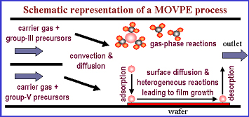
Introduction of simulation and modeling into
development of MOVPE technology becomes more and more intensive in the last years. Modeling
may be used for both process and reactor optimization purposes. Besides the description
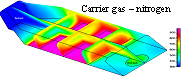
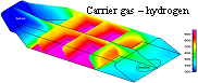
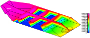
of transport phenomena (flow, heat, species), an adequate chemistry model is necessary to predict
deposition rates and uniformities and layer compositions. A surface chemistry model should be
able to predict epitaxial growth on the wafer as well as parasitic deposition on the reactor
inner surfaces, which occurs under kinetically limited conditions.
|
We developed an integrated approach to simulation of III-V materials growth by MOVPE.
The low temperature kinetic effects are described using a general mechanism – the blocking
of group III species adsorption sites by methyl radicals. The mechanism is based on experimental
data on the decomposition of group III metal-organic precursors on III-V semiconductor surfaces.
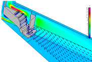
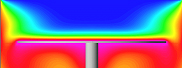
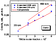
Deposition at intermediate temperatures that occurs under mass-transport limited growth
conditions necessitates detailed modeling of transport processes accounting for reactor
geometry features. These conditions are characteristic for MOVPE of group III arsenides
and phosphides and the modeling results for these materials can be found in the reference list.
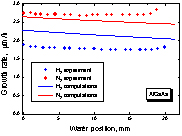
Another advantage of the formulated model is its ability to predict the growth rate and
composition of the epitaxial layers under the conditions when the desorption of species from
the surface is the rate limiting process. This is particularly important for the regimes
of thin strained quantum well growth. The developed models describe growth of the epilayers
in the Al-Ga-In-As-P system used for growing heterostructures for light emitting diodes,
solar cells, laser diodes, high-electron mobility transistors, hetero-bipolar transistors
and vertical cavity surface emitting lasers. These structures include GaAs, InP, AlGaAs,
InGaAs, and InGaP layers.
References on Models and mechanisms
2001
On low temperature kinetic effects in Metal - Organic Vapor Phase Epitaxy of III-V compounds.
R.A. Talalaev, E.V. Yakovlev, S.Yu. Karpov, Yu.N. Makarov.
Journal of Crystal Growth, Vol.230, p.232-238, (2001).
2000
Quasi-thermodynamic models of surface chemistry: application to MOVPE of III-V ternary compounds.
S.Yu. Karpov, E.V. Yakovlev, R.A. Talalaev, Yu.A. Shpolyanskiy, Yu.N. Makarov, S.A. Lowry.
Electrochemical Society Proceedings, Vol. 2000-13, p.723-730, (2000).
1997
Advanced mathematical models for simulation of radiative heat transfer in CVD reactors.
F.Durst, L.Kadinski, Yu.N.Makarov, M.Schafer, M.G.Vasil’ev, V.S.Yuferev.
Journal of Crystal Growth, Vol.172, p.385-395.
1995
Development of advanced mathematical models for numerical calculations of radiative heat transfer in metalorganic chemical vapour deposition reactors.
L.Kadinski, Yu.N.Makarov, M.Schafer, M.G.Vasil’ev, V.S.Yuferev.
Journal of Crystal Growth, Vol.146, p.209-213, (1995).
References on III-V growth in the Horizontal and Planetary Reactors
2003
Advances in the modeling of MOVPE processes.
S. Yu. Karpov.
J. Crystal Growth, Vol.248, p.1-7, (2003).
2001
Detailed modeling of Metal Organic Vapor Phase Epitaxy of III-V ternary compounds in production-scale AIX 2400G3 Planetary Reactor.
E.V. Yakovlev, Y.A. Shpolyanskiy, R.A. Talalaev, S.Y. Karpov, Y.N. Makarov, T. Bergunde, and S.A. Lowry.
Electrochemical Society Proceedings, Vol. 2001-13, p.292-300,(2001).
2000
Comprehensive reactor-scale modeling of III-V ternary compound growth by MOVPE.
E.V. Yakovlev, R.A. Talalaev, S.Yu. Karpov, Yu.A. Shpolyanskiy, Yu.N. Makarov, S.A. Lowry.
Mat. Res. Soc. Symp. Proc., Vol.616, p.153-158, (2000).
Modeling and experimental verification of transport and deposition behavior during MOVPE of Ga1-xInxP in the Planetary Reactor.
M. Dauelsberg, L. Kadinski , Yu.N. Makarov , T. Bergunde , G. Strauch, M. Weyers.
Journal of Crystal Growth, Vol.208, p.85-92, (2000).
1997
Heat transfer and mass transport in multiwafer MOVPE reactor: modelling and experimental studies.
T.Bergunde, M.Dauelsberg, L.Kadinski, Yu.N.Makarov, M.Weyers, D.Schmitz, G.Strauch.
Journal of Crystal Growth, Vol. 170, p.66-71, (1997).
Process optimisation of MOVPE growth by numerical modelling of transport phenomena including thermal radiation.
T.Bergunde, M.Dauelsberg, L.Kadinski, Yu.N.Makarov, V.S.Yuferev, D.Schmitz, G.Strauch, H.Jurgensen.
Journal of Crystal Growth, Vol.180, p.660-669, (1997).
Modelling and process optimization in a radial flow multiwafer MOVPE reactor.
T.Bergunde, M.Dauelsberg, L.Kadinski, Yu.N.Makarov, G.Strauch, H.Jurgensen.
Society Proceedings, Vol. 97-25, p.230-237, (1997).
1995
Transport and reaction behaviour in Aix-2000 Planetary MOVPE reactor.
T.Bergunde, D.Gutsche, L.Kadinski, Yu.Makarov, and M.Weyers.
Journal of Crystal Growth, Vol.146, p.564-569, (1995).
Algorithms and Models for Simulation of MOCVD of III-V Layers in the Planetary Reactor.
T.Bergunde, M.Dauelsberg, Yu.Egorov, L.Kadinski, Yu.N.Makarov, M.Schafer, G.Strauch, M.Weyers.
Simulation of Semiconductor Devices and Processes, Vol.6, edited by H.Ryssel, P.Pichler, p.328-331, (1995).
1994
Modelling of growth in a 5x3 inch multiwafer metalorganic vapour phase epitaxy reactor.
T.Bergunde, M.Dauelsberg, Yu.Egorov, L.Kadinski, Yu.N.Makarov, M.Schafer, G.Strauch, M.Weyers.
Journal of Crystal Growth, Vol. 145, p.630-635, (1994).